
Skip to content
Bits&Chips
×
×
About
Memberships
Advertising
Magazines
Videos
Contact

Log in

Analysis

Nanoimprint lithography won’t compete with EUV anytime soon

4 November 2025
Paul van Gerven
Editor at Bits&Chips
Reading time: 3 minutes

A new analysis refutes Canon’s claims that nanoimprint lithography can take on EUV.

Nanoimprint lithography (NIL) won’t be able to compete with EUV lithography in the foreseeable future. A handful of issues “without any clear way forward” stand in the way of a debut in leading-edge chip manufacturing, according to a report by Semianalysis.

NIL involves pressing a mask imprinted with the circuit pattern on a resist-coated wafer area, like a stamp. The technique was once considered a potential successor to DUV immersion lithography, but the semiconductor industry threw its weight behind EUV instead.

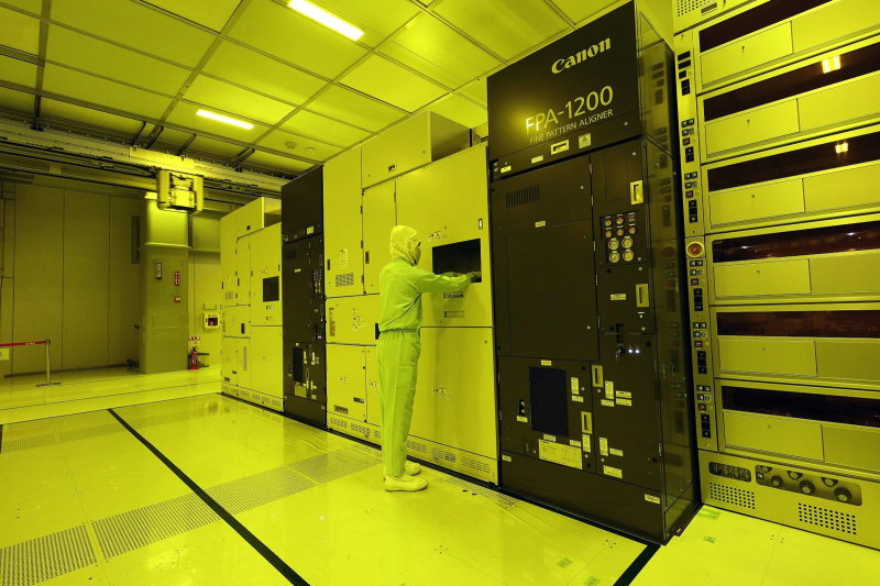
Canon never gave up on the technology. Initially through in-house research, later bolstered by the acquisition of the US startup Molecular Imprints in 2014, the Japanese have been developing a potential alternative to EUV for over twenty years. They launched their first NIL tool in 2023, claiming the machine is capable of producing 5nm and more advanced chips at a considerably lower cost than EUV. Canon has said it wants to sell 10-20 units annually in two to four years.

Clustered

On paper, NIL has indeed potential for leading-edge chip patterning. It’s one of few technologies that can reach ‘EUV resolutions’ in the first place without any obvious other characteristics that would make it impractical for high-volume manufacturing. NIL tools are less complex, cheaper to manufacture and use less power than EUV scanners to boot. However, after taking inventory of technical hurdles, Semianalysis concludes that NIL can’t deliver at the scale or robustness required for leading-edge logic and memory manufacturing.

One of the most fundamental problems is mask (or “template”) durability. Because the NIL process involves physical contact (pressing into the resist on the wafer), the mask’s fine 3D features are subject to mechanical stress, breakage and particle generation. According to Semianalysis, current mask lifetimes are in the order of fifty wafers in real-world use, despite optimistic claims of more than ten times that. This results in excessive mask and inspection costs.

A second key issue is overlay, or the ability to align a pattern to prior layers on the wafer. NIL overlay error is about four times larger than needed, according to analyses. Metrology improvements could offer a reprieve but would require an overhaul of the architecture of Canon’s NIL tool.

Even if the mechanics of mask life and overlay were solved, NIL still faces challenges in patterning fidelity: the creation of sharp, smooth features on the mask/template at the nanometer scale is difficult. Roughness in the mask or template translates into line-edge roughness or degradation in the printed features, which can lead to wire shorts, leakage or performance losses. The ecosystem of resist, imprint materials, curing and pattern transfer (etch/deposition) is less mature for NIL than for optical lithography, which benefits from decades of accumulated process know-how.

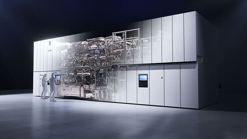
Finally, although NIL’s patterning tool cost and power consumption may look favorable, throughput remains weak compared to EUV scanners. For example, the Canon NIL tool is quoted at about 25 wafers per hour, or about 100 wafers per hour for a clustered setup. Today’s EUV scanners are at least twice as fast, and ASML targets 400-500 wafers per hour in a few years.

Unwarranted

The physics of contact imprinting, the fragility of masks/templates, overlay limitations, pattern-stack maturity and throughput constraints all combine to make NIL unsuitable and not cost-effective for production at the advanced nodes, where EUV will continue to reign supreme – possibly until the lithography roadmap hits a wall.

That’s not to say that NIL is useless. There are plenty of applications where it could succeed, particularly when overlay and defectivity requirements are lower, such as in less advanced logic/memory nodes, or specialty patterning of micro-optics, MEMS, sensors and metalenses. But the blanket claim that NIL will replace EUV for leading-edge nodes is unwarranted at present.

Top image credit: Canon
Related content

ASML expects high-NA EUV to reach production-grade availability by year-end

Machines that think: embodied intelligence

Top jobs
Your vacancy here?
View the possibilities
in the media kit
Events
Courses
Headlines
  • Romanian software branch now fully in Sioux’s hands

    7 September 2026
  • Chinese court freezes Nexperia assets

    2 September 2026
  • ASML expects high-NA EUV to reach production-grade availability by year-end

    2 September 2026
  • Intel signals external customer wins for 14A foundry process

    2 September 2026
  • Nexperia reports Q2 revenue and profitability growth

    31 August 2026
  • Delmic automates nanoscale measurements

    31 August 2026
  • Dutch chip industry tops 46 billion euros in 2025

    27 August 2026
  • Besi faces longer wait as SK Hynix pushes hybrid bonding to HBM5

    26 August 2026
  • Nexperia China cuts European wafer ties with domestic 12-inch production

    25 August 2026
  • Iran war deadlock gave ASML reprieve from US China crackdown

    21 August 2026
  • Taiwanese engineers boost 2D transistor performance

    18 August 2026
  • Nokia retools NXP’s Chandler fab for InP manufacturing

    17 August 2026
  • Global semiconductor market doubles in H1 2026

    11 August 2026
  • Samsung reportedly expects high-NA EUV insertion at 1nm node

    11 August 2026
  • Nanya set to become ASML’s newest EUV customer

    11 August 2026
  • Musk hints at free-electron laser EUV source tech for Terafab

    10 August 2026
  • Zeiss dismisses bottleneck concerns

    4 August 2026
  • SK Hynix raises annual chip investment to record $31B

    3 August 2026
  • Wafer fab equipment market heads for $220B by 2031

    3 August 2026
  • NXP explores acquisition of US edge AI firm Ambarella

    3 August 2026
Bits&Chips logo

Bits&Chips strengthens the high tech ecosystem in the Netherlands and Belgium and makes it healthier by supplying independent knowledge and information.

Bits&Chips focuses on news and trends in embedded systems, electronics, mechatronics and semiconductors. Our coverage revolves around the influence of technology.

Advertising
Subscribe
Events
Contact
Follow us on
High-Tech Systems Magazine (Dutch)
(c) Techwatch bv. All rights reserved. Techwatch reserves the rights to all information on this website (texts, images, videos, sounds), unless otherwise stated.
  • About
  • Memberships
  • Advertising
  • Videos
  • Contact
  • Search
Privacy settings

Bits&Chips uses technologies such as functional and analytical cookies to improve the user experience of the website. By consenting to the use of these technologies, we may capture (personal) data, unique identifiers, device and browser data, IP addresses, location data and browsing behavior. Want to know more about how we use your data? Please read our privacy statement.


Give permission or set your own preferences

Functional Always active
Functional cookies are necessary for the website to function properly. It is therefore not possible to reject or disable them.
Voorkeuren
De technische opslag of toegang is noodzakelijk voor het legitieme doel voorkeuren op te slaan die niet door de abonnee of gebruiker zijn aangevraagd.
Statistics
Analytical cookies are used to store statistical data. This data is stored and analyzed anonymously to map the use of the website. De technische opslag of toegang die uitsluitend wordt gebruikt voor anonieme statistische doeleinden. Zonder dagvaarding, vrijwillige naleving door je Internet Service Provider, of aanvullende gegevens van een derde partij, kan informatie die alleen voor dit doel wordt opgeslagen of opgehaald gewoonlijk niet worden gebruikt om je te identificeren.
Marketing
Technical storage or access is necessary to create user profiles for sending advertising or to track the user on a site or across sites for similar marketing purposes.
  • Manage options
  • Manage services
  • Manage {vendor_count} vendors
  • Read more about these purposes
View preferences
  • {title}
  • {title}
  • {title}

Your cart (items: 0)

Products in cart

Product Details Total
Subtotal €0.00
Taxes and discounts calculated at checkout.
View my cart
Go to checkout

Your cart is currently empty!

Start shopping

Notifications